
In order to see if the design is working before committing to a full build in the FPGA I wanted to simulate it to see if it could render just a few pixels and return sensible pixel locations. There are of course lots of different complicated ways of doing this, some quite elaborated, but I just wanted to functionally verify the design in the shortest amount of time (this is a hobby project after all). So, I opted o use Xilinx BFMs. These are IP cores that can generate different kinds of traffic on AXI buses. Here’s the testbench that I created:

You can see that there are are few basic blocks like a clock generator and a reset block that are needed in any design. The important block that we added is the one that is selected in the middle, it is a an AXI-Lite master block. This can be controlled by Verilog statements to send out traffic on its master bus port. This bus connection is then routed through an interconnect to the vertex pump master and to the pixel block ram. This way we can set the contents of the block ram and configure the vertex pump from the same bus. The output of the vertex pump is an AXI-Stream with the raw pixels. They are transformed into screen coordinates by the screen transform block. The point painter then proceeds to draw these onto the screen. The output of the point painter is an AXI-Full master bus. This bus would normally by connected to the main memory of the system where the pixel buffer lives. In this testbench, I hooked it up to a slave AXI-Full BFM. This will simply consume the bus operations and do the handshaking so we can see the IPs in action.
In the testbench, I first wrote a raw vertexes into the vertex BRAM like so:
gpu_testbench_i.cdn_axi_bfm_0.cdn_axi4_lite_master_bfm_inst.WRITE_BURST(
 32'hC0000000, mtestProtection, 0, 4, response );
 gpu_testbench_i.cdn_axi_bfm_0.cdn_axi4_lite_master_bfm_inst.WRITE_BURST(
 32'hC0000004, mtestProtection, 0<<10, 4, response );
 gpu_testbench_i.cdn_axi_bfm_0.cdn_axi4_lite_master_bfm_inst.WRITE_BURST(
 32'hC0000008, mtestProtection, 5<<10, 4, response );
Address 0 corresponds to location 0 of the BRAM, address 4 corresponds to location 1 and so on. So this first vertex has these coordinates: (0, 0, 5). (The data is shifted 10 bits left because I used 10 bits for the fraction in the HLS blocks). Afterwards, I set up an ran the Vertex pump:
// Set up Vertex pump
 gpu_testbench_i.cdn_axi_bfm_0.cdn_axi4_lite_master_bfm_inst.WRITE_BURST( // FB address
 32'h44A00018, mtestProtection, 32'h00000000, 4, response );
 gpu_testbench_i.cdn_axi_bfm_0.cdn_axi4_lite_master_bfm_inst.WRITE_BURST( // Number of vertexes
 32'h44A00010, mtestProtection, 32'h00000006, 4, response );
 gpu_testbench_i.cdn_axi_bfm_0.cdn_axi4_lite_master_bfm_inst.WRITE_BURST( // Start
 32'h44A00000, mtestProtection, 32'h00000001, 4, response );
Running the sim, this is how the BFM looks when it’s sending out the write transfers to the BRAM:

After the BRAM controller, these are the BRAM signals when accepting the writes:
We can see that two 0’s are written to address 0x0000 and 0x0004, followed by a 0x1400 at address 0x0008. These are the x,y and z coordinates of the first vertex. Next, lets look at the vertex pump running:

Looks good! It’s reading the BRAM data and pumping it out on the AXI-Stream bus. It’s kind of hard to see if the data coming out is correct since its a single 64 bit vector. Lets try splitting it into x,y,z at the input of the screen transform and see what location the screen transform thinks it should be at on the display:

So an input 0,0,5 got turned into (400,300). That’s right in the middle of the frame! Seems like it’s working then. I pumped a few more pixels through at different locations and it looks solid:
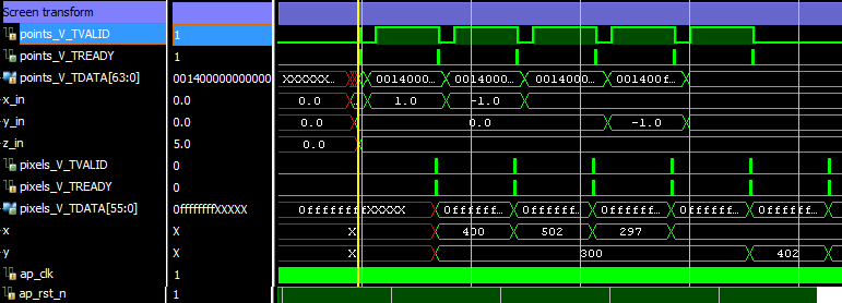
These are the pixels it converted:
(0,0,5) -> (400,300)
(1,0,5) -> (502,300)
(-1,0,5) -> (297,300)

(0,0,5) -> (400,300)
(0,-1,5) -> (400,402)
(0,2,5) -> (400,95)
Seems like we are ready to try it out on real HW.