GPU Project 08 – Point cloud rendering in FPGA

After successfully running the simulation, its time to see how the rendering works on the real HW. And as always, SW needs to be written to get the HW to know what to do. In this case, I will be loading the vertex data of a cube into memory to see it transformed, and then experiment with the same teapot data that I used in the C# version the app.

Continue reading

GPU Project 07 – Simulating the design

In order to see if the design is working before committing to a full build in the FPGA I wanted to simulate it to see if it could render just a few pixels and return sensible pixel locations. There are of course lots of different complicated ways of doing this, some quite elaborated, but I just wanted to functionally verify the design in the shortest amount of time (this is a hobby project after all). So, I opted o use Xilinx BFMs. These are IP cores that can generate different kinds of traffic on AXI buses. Here’s the testbench that I created:

Continue reading

GPU Project 06 – HLS IPs

Hi!

Well, due to being very busy at work I hand’t had a chance to actually post progress on the project, but we most definitely have progress! If you have been following these posts, you can see that last time we sketched out the overall architecture of the video card. 

In order to render point clouds we only need the three blocks that are highlighted. Basically, a mechanism for pulling in raw vertexes from memory, a block that can transform the 3d points to a 2d screen space, and a block that can take those points and draw them on a frame buffer. So, here they are!

Continue reading

GPU Project 05 – Sketching the RTL

So, the time has finally arrived. Time to tackle the GPU in HW! So, a quick disclaimer: since this is a hobby project I will use HLS to quickly iterate designs and reach a functional RTL. All of the blocks will be designed considering that they are meant for RTL and (given enough time) could be replaced by hand coded VHDL/Verilog without too  much hassle. This is the architecture that I am envisioning:

Continue reading

GPU Project 04 – Simple 3D object parser

So, last week we got a basic projection algorithm in place. We “rendered” the vertices of the cube into a bitmap, but we barely know got it see it working. We definitely need something more complicated to see it operating. One option is to just try to hard code a list of larger vertices that describe a more complex object, but doing that by hand is definitely cumbersome, inexact and prone to errors. Instead, I decided to rely on the vast world wide web and find several 3d objects that I could use. It turns out that there are millions of such objects in many, many websites, but all of these are in different formats. After some hunting, I setted on using a .obj format. These are the reasons:

  • Plain ASCII format: Can’t beat this when it comes to ease of parsing
  • No compression
  • Simple 3d object structure.
  • Vertexes and faces are separate.


Continue reading

GPU Project 03 – World and space

So, now that we have a way of showing images, let start digging into how we will actually generate the images that we will show. The basic idea is that a 3D scene is formed by a digital representation of the objects that we want to show, and that a video card transforms this information into a 2d image that we can see on a screen. The first side is usually the task of really 3d designers, game creators, artists and whismy programmers that create collections of points, lights and textures that represent a 3d object. Since we are starting from scratch, we will start by trying to render a collection of points in space. These points will simply be a set of (x,y,z) points in the world. I always like to use coordinates the way PC game designers use them:

Continue reading

GPU Project 02 – Basic frame buffer and DMA code

The idea in the previous post was to create a suitable framebuffer display circuit that could be used as a generic part of the video card that sends the content of the framebuffer to a monitor or tv. After I moved to a different computer I realized how inconvenient it is to have a project slaved to a particular set of board files. These are not copied with the project so I decided to remove the dependency with the board files and synthesize again. (The updated Vivado project and bitstream are attached).

So, with the FPGA fabric in place we needed to create a basic application that runs on the Zynq’s ARM to write to the framebuffer and configure the VDMA block. This will work to verify that the output VDMA and VGA circuit is working correctly.

So, first thing first. We need to get a bare metal application working on the board. I exported the .HDF file from the Vivado project and fired up Xilinx SDK.

Continue reading

GPU Project 01 – Zybo is in!

So, after waiting anxiously for a few days, it’s finally in. The box it arrived in was rather large, but really light. I was worried that there was nothing in it:DSC_0186_m

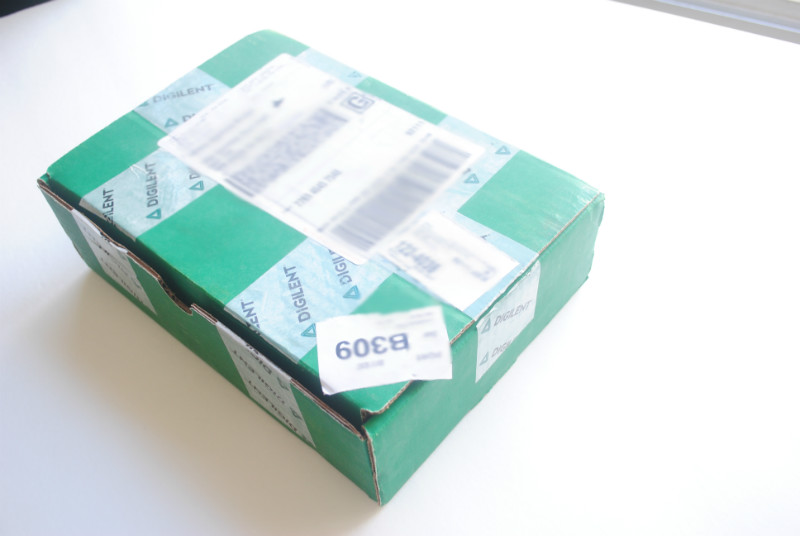
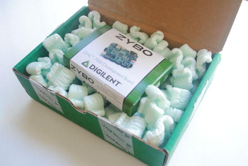
After opening it up, I can see that the real board is inside a much smaller box:

DSC_0188_m

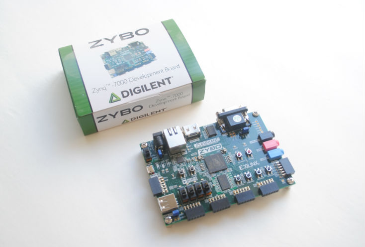
And finally taking out of the box:

DSC_0193_m

So, time to roll up our sleeves! I installed Vivado 2016.2 with the free Webpack edition. Compared to the normal System Design edition it is mostly the same, but restricted to only a few devices. Thankfully for me, this Zybo board is one of the free devices supported by the free edition.

So, first thing first. I need to start creating a project that pumps out an image from a buffer in DDR to a display. Remember the block diagram from last post? We’ll focus on this for now:

GPU01_video_out

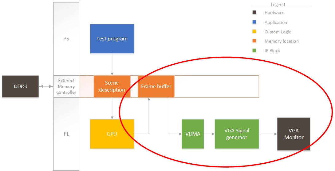
Right now we won’t have any fancy GPU rendering the image, so I’ll have the ARM on the Zynq draw some pixels to see that it’s working properly. So, for this design, I instantiate the PS section in Vivado and add three clocks to the system:

  • AXI clock. I will use this for all the AXI-Lite interfaces to control registers, etc.I set this to 50MHz. Could be slower, but seems like a good starting value.
  • Memory clock. I will use this to connect all the VDMAs and interfaces that need to talk to memory. I set this to 166MHz. Don’t ask why, but this always seems to work in all my designs.
  • Video clock. This will be the pixel clock. Video interfaces will be connected at this speed. (40MHz). I chose this speed since I will be generating an output VESA 800×600 image stream at 60fps.

After adding in the clocks (generated by the PS section for simplicity), I also added a VDMA. This needs to be connected through an AXI protocol converter, since the PS block only supports AXI3, but everything else is AXI4. This first VDMA will pull data from the framebuffer into the logic. I then connected the VDMA to an output AXI to video out block. This block can directly drive a VGA port. The output video block requires some timing, so we also add a timing generator. The timing generator will run in master mode, clocking video for an 800×600 resolution.

GPU01_block_design

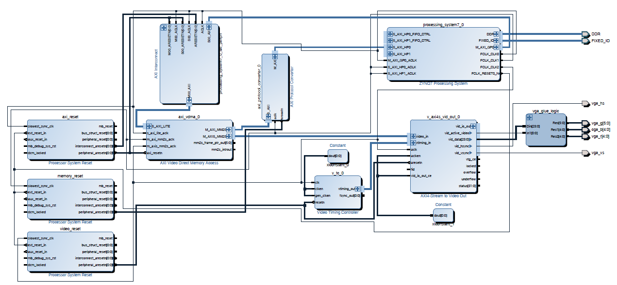
Click on the image to expand it in case (most likely) things are squished in the browser. I will be posting the source files at the end of all my posts.

I added the constraints from the master XDC file on the Digilent website for the VGA port only. The next step is to run full synthesis/route/bitstream generation and see if we have something that is not broken. If that’s good then we’ll program the FPGA and start working on the ARM code that will configure the VDMA and write a test frame. Note that I’m uploading the design files as I’m working so things might be broken.

Goodies:

Vivado block design

Project XDC files

Time to run synthesis, see you next time!