
The idea in the previous post was to create a suitable framebuffer display circuit that could be used as a generic part of the video card that sends the content of the framebuffer to a monitor or tv. After I moved to a different computer I realized how inconvenient it is to have a project slaved to a particular set of board files. These are not copied with the project so I decided to remove the dependency with the board files and synthesize again. (The updated Vivado project and bitstream are attached).
So, with the FPGA fabric in place we needed to create a basic application that runs on the Zynq’s ARM to write to the framebuffer and configure the VDMA block. This will work to verify that the output VDMA and VGA circuit is working correctly.
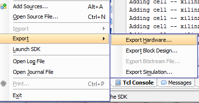
So, first thing first. We need to get a bare metal application working on the board. I exported the .HDF file from the Vivado project and fired up Xilinx SDK.
In Xilinx SDK I generated a new project based on the Hello World template and referenced the HDF I exported from Vivado for the hardware platform. I built the projects and got ready to test. One useful thing to remember is that Eclipse has built in serial port capabilities so you don’t need to install a terminal application. To enable the built in serial port I went into the debug configurations window and set up the STDIO connection tab with the correct settings: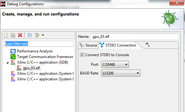
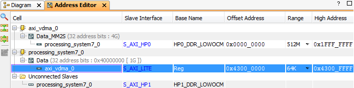
I ran the application and verified that the hello world app was working. Next up, time to configure the VDMA. We need to make sure we know the base address at which the VDMA lives. We can figure this out by going to the Vivado project and inspecting the offset address for the vdma:
Now, time to write some code to configure the block. This boils down to inspecting the fields of the registers and setting it up with the configuration that we want. The user guide for the VDMA can be found here:
https://www.xilinx.com/support/documentation/ip_documentation/axi_vdma/v6_2/pg020_axi_vdma.pdf
On page 14 we can find the register map and figure out a configuration that we want. For now, we want the VDMA to pump out 800×600 pixels with 4 bytes per pixel to align things to 32 bit words. I created a couple of helper functions to help when writing to hardware:
uint32_t reg_read(void*device, uint32_t offset){
	volatile uint32_t *ptr;
	uint32_t ret;
	ptr = (uint32_t*)(device + offset);
	ret = *ptr;
	return ret;
}

void reg_write(void*device, uint32_t offset, uint32_t data){
	volatile uint32_t *ptr;
	ptr = (uint32_t*)(device + offset);
	*ptr = data;
}
The sequence to set up the VDMA consists of specifying the frame buffer address, the operating mode, the width, stride, and height:
// Clear errors
reg_write(localvdma, 0x04, 0x7090);

// Set framebuffer
reg_write(localvdma, 0x5C, fb_address + (width*channels*height*1));

// Set up mode
reg_write(localvdma, 0x00, 0x00000003); // RS=1, genlock off

// Set screen size
reg_write(localvdma, 0x58, (width * channels)); // Stride
reg_write(localvdma, 0x54, (width * channels)); // H size
reg_write(localvdma, 0x50, height); // V size
So, now that we have a VDMA that is constantly pumping the framebuffer out through the VGA interface we need to write some data to the framebuffer so that we can see something interesting on the display. I made a small function that creates vertical and horizontal gradients in a local framebuffer, then copies the data to a second framebuffer that is used by the VDMA:
void copy_frame(){
	Xil_DCacheDisable();
	memmove( (void*)display_buffer_hw, (void*)display_buffer_sw, IMAGE_WIDTH * IMAGE_HEIGHT * 4 );
	Xil_DCacheEnable();
}
Note that I had to disable the DRAM cache because if not the memove operation does not write the all the data to the external DDR (which leaves horrible streaks).
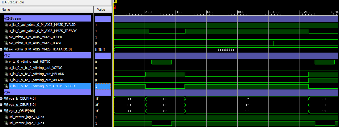
I ran this code and also added in a few chipscope probes to see the data coming out of the VDMA and then going out of the VGA controller:
Now, time to verify that all that is working correctly. I realized that my TV does not have a VGA input. Since I had already done all the work of getting this to work with VGA and did not want to put an HDMI IP core in the fabric I went to Fry’s and bought a VGA to HDMI converter:

These are getting harder and harder to find as time goes by, but I managed to find one under $15 USD. I plugged this into my TV and this is what I saw:
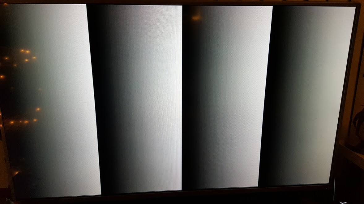
I’m pretty sure my wife must have thought that it was odd for a grown man to be so exited over such a boring sight! 🙂 However, this means that we have a working video pipe and anything that we write to the DDR framebuffer will appear on the display. Looks like we are on track!
Cheers, and see you next week.
– Alfredo
Goodies:
Note: The bitstream is precompiled and can be found in the .runs\impl_1 directory in the project.
Hi Alfredo,
few time ago I bought a Zybo board and now I’m learning to use it following some tutorials. I’ve found your project and it is very interesting and useful because I’d like to use zybo for video processing.
I use the last version of Vivado (2016-4): when I open you project it migrates and updates all the IPs. But when I verify the block design occurs an error related to different data width between VDMA (4 bytes) and VideoOut (3 bytes). I’ve tried to insert an AXIS Data Width converter between VDMA and VideoOut and the bitstream seems to be generated correctly. But when I export to SDK and program to FPGA no VGA signal is detected by the monitor!
If I try your pre-generated bitstream it works correctly.
Do you have any idea? Did you have tried with last version of Vivado?
Thank you very much!
Sergio
Hi Sergio,
The mismatch is because the VMDA is operating on 32 bit words, and the video out is using 24 bits only. In theory you should be able to just ignore the warning (at least in 2016.2 you get this message as a warning only “Bus Interface property TDATA_NUM_BYTES does not match between /vga_video_out/video_in(3) and /axi_vdma_0/M_AXIS_MM2S(4)”). If the design does not work after adding the AXIS data width converter, it is likely that the the TLAST and TUSER signals in the converter IP are not enabled. These are used for video synchronization and the video out IP will ignore the input stream unless it has both of these (TUSER signals the first pixel of the frame, TLAST signals the last pixel of each line). I will probably migrate to 2016.4 in the next month for the following posts to keep up to date.
-Alfredo
Hi Alfredo,
thank you for the answer.
I’ve resolved introducing a slice IP instead of AXIS Data Width converter!
Regards
Sergio